The Goal
The first stage of my Audio pipeline is responsible for getting audio data from a host and turning it into a usable format. As mentioned last time, I decided to base this stage on the CP2615 which essentially does exactly what I want. I’ve decided to use this chip rather than writing my own USB driver on a Raspberry Pi or Artik 510 board to get started; in the future, this may be a place that I make some big changes, but for now, I just want audio samples.
KiCad
I decided to use KiCad on this project because it is free and I’ve known people who have used it in the past. I’ve used Eagle before, but now that they’re a subscription service, I’m not really interested in using it at this time.
In terms of getting started, the process was pretty easy; I started a new project, and immediately opened the
schematic to get started. Since KiCad is really a suite of tools, the schematic editor is called Eeschema,
and it’s pretty solid! The default parts library is pretty solid, and I was able to pretty quickly get the
hang of things. I started by adding the I/O pieces.
Schematic Design
I/O
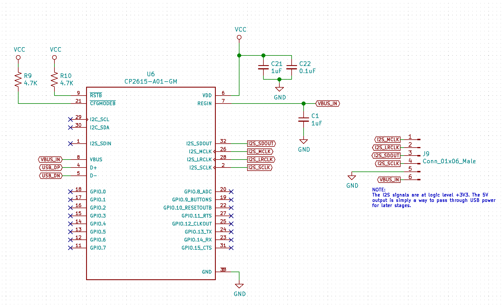
Since the main component of this board is the CP2615, which takes USB as input and outputs I2S, the I/O was pretty well set for me. For the USB 2.0 interface, I chose a USB B Micro connector, which is what the reference design also used. I was initially tempted to drop the ESD protection diodes, but decided that it wasn’t worth the risk, even though I felt pretty safe without them. I also borrowed from the CP2615 reference design and used the SP0503 diode array.
For the output, I chose to simply use 0.100" (2.54mm) headers; they’re easy to use, I don’t think I need anything fancy in terms of signal integrity, and I have plenty of space (I have as much as I want!).
One thing I found fairly unintuitive was the way that KiCad/Eeschema deals with multiple pages. Eeschma uses the concept of “hierarchical sheets”, which takes a little bit of getting used to. I’m still not 100% comfortable with it, but I imagine that as I use it more, I will get more comfortable.
Power
When I first started down this path, I wasn’t sure if I wanted to drive headphones or speakers with this audio design. I initially wanted to add DC power at this stage, thinking it would give me more flexibility down the road. I designed some small power circuitry to create 5V and 3.3V on the board, and set up the CP2615 to use these voltages rather than the USB 5V VBUS.
As I spent more time thinking about it, I realized that driving headphones was much more practical. First, I only really have one set of PC speakers that I could drive, which isn’t that interesting. I have (and have access to) many different types of headphones. Bonus: the neighbors won’t be able to hear my headphones unless something goes drastically wrong. The final bit was that driving actual speakers can involve some serious power (hundreds of watts). Considering that I haven’t spent much time designing circuits and PCBs at those power levels, I decided that I wanted to start just by driving my headphones.
In theory, converting from external power to USB power was simple: remove the power circuitry and hook up the CP2615 to USB. In practice, however, I messed this up not once, but twice. The CP2615 can create its own 3.3V reference voltage from a 5V VBUS input, which is convenient. Mistake 1: Unfortunately, I accidentally tied my 5V and 3.3V together, which I noticed after the PCBs arrived, but before I actually populated it. Mistake 2: On a similar note, I connected the REGIN pin of the CP2615 directly to the 3.3V output voltage, which again meant that the chip would never be able to create power.
Result
The schematic is quite simple, embarrassingly so considering I messed it up twice. The interesting stuff is here; what you can’t see is the USB input and ESD protection diodes.
PCB Design
After the schematics were finished, I then switched to the PCB design. The KiCad tool for this is called
Pcbnew, and also works reasonably well. The autorouter was pretty terrible, which I was a bit surprised
by, given that my circuit was pretty simple (1 IC and about 5 passive components), but in general I believe
that autorouters are pretty terrible, so I wasn’t upset.
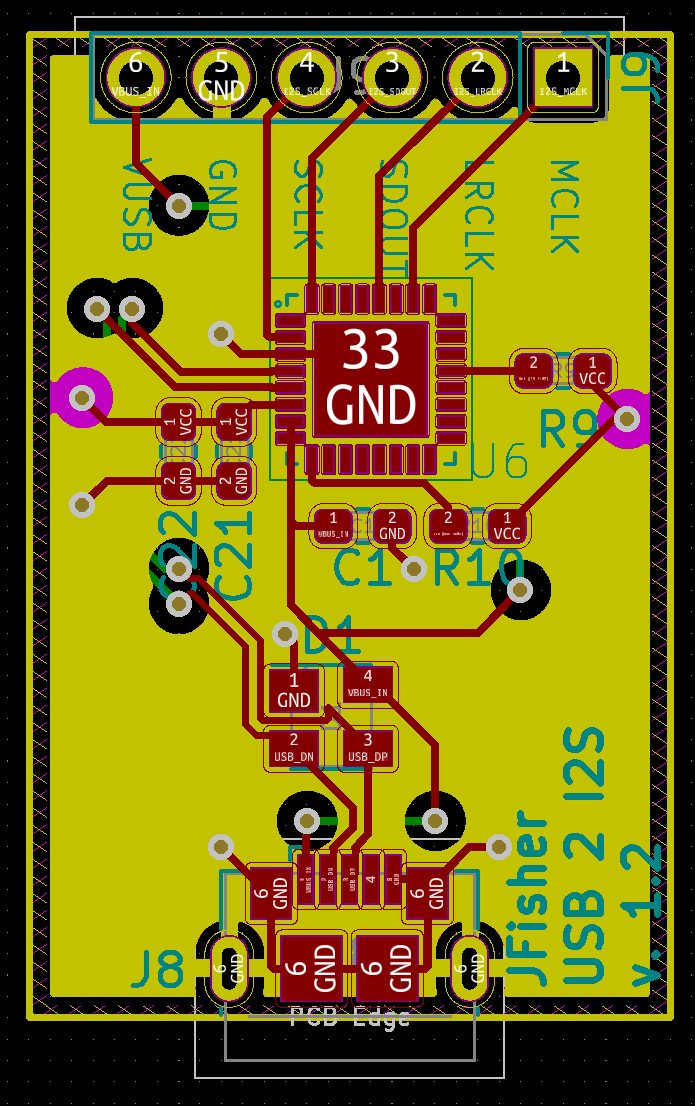
The first step was to assign footprints to the various components I had selected in the schematic. I decided to use 0603-sized passives, since I felt confident that if need be, I could solder those by hand. For the CP2615, though, I had to up my game. The CP2615 is only available in a QFN package, with a large ground pad on the bottom. Although there are videos on YouTube for soldering QFN using an soldering iron, this was solidly beyond my capabilities. It was time for a toaster oven.
While there are some reflow ovens available on things like eBay and Amazon, the ones I saw were all fairly crappy looking, and ultimately not something I needed. I’ve used toaster ovens before for small PCBs, and decided to go that route again. While I briefly considered trying to go above and beyond on this, I ended up just spending $18 on the cheapest Black & Decker toaster oven on Amazon and hoping for the best.
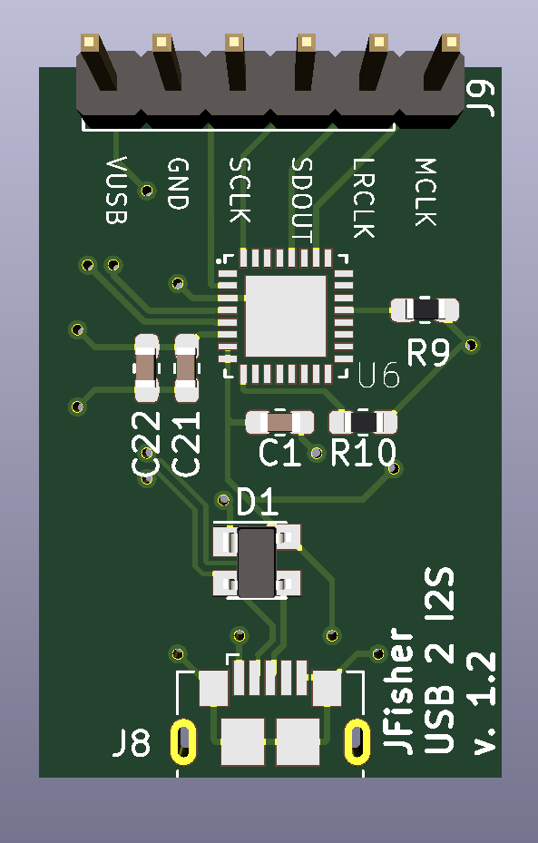
Once I had the footprints selected, the rest of layout was fairly straightforward. I used the Pcbnew “differential routing” feature to route the USB data lines, which I found pretty good and saved a lot of work trying to do that manually. In general, the process of laying out this board was straightforward; a few vias and a couple of pours and I was done! The 3D viewer was pretty fun to see what things would (ideally) look like once the boards arrived.
Layout
Rendering
PCB Fabrication
Once I had my PCB designed, I had to figure out where to get it made. I’ve heard good things about OSHPark
and Seeed Studio, so it was mostly a tossup. I decided to
go with OSHPark. Their website was surprisingly easy to use; I dragged-and-dropped my kicad_pcb file onto
the browser and…. was basically done. And $8.60 for 3 boards was a pleasant surprise. I opted for the USPS
basic shipping, since I was in no rush, and I was done.
Summary & Lessons Learned
Well, as I write this, I am awaiting my v3 board to arrive. The biggest lesson for me is to double and triple check my work. I was too careless in quickly checking my work, and ultimately have had to sacrifice time because of it. I’ve been able to use this time to start working on the next board (DAC), where I intend to be more cautious.
In good news, my toaster oven worked very well! I bought some low-temperature solder paste, and populated the v2 board once it came in and that worked remarkably well. The process was quick and relatively simple. Granted, the board didn’t work because of my error, so it is possible that one or more of the solder joints was bad, but it looked good to the naked eye at least!
Next
Once my new board arrives, I will once again try to get that working. The hope is to hook up the oscilloscope and see I2S data being clocked out of the output of the board. At that point, I will focus on getting the DAC board finalized and send off to be made!