Audio DAC: Part III
When I left off last time, I needed to make some changes to my audio DAC board. This was because in order to create a valid clock rate, I needed to expose the PCM5242 GPIOs, as well as the a software control interface.
Hardware Redesign
Software Control Interface
The PCM5242 supports either SPI or I2C for a software control mode. I chose to expose the I2C interface for a couple of reasons:
- It’s 3 wires (SDA, SCL and GND) vs. 5 for SPI (MISO, MOSI, CLK, SS, GND).
- I don’t have real speed requirements (100kHz / 400kHz is plenty fast enough).
One sort of annoying thing is that I needed to add two more passives: pull-ups for both the SDA and SCL lines. This is because the I2C protocol is open-drain. While this isn’t a cost consideration, it’s annoying because I am currently doing my reflow soldering using the cheapest toaster oven I could find on Amazon!
Exposing Pins
I decided that, given the issue that required this board respin, I should bring out as many pins as I seemed likely to ever want. I broke out the MODE pins (used to select the control mode between Hardware, I2C and SPI). I also brought out the GPIO3-GPIO6 pins on the PCM5242. All of these can be configured in fun ways, and my intention was to use them to create a valid I2S clock.
Ordering
After a quick double-check of my routing, I ordered the boards. I felt fairly confident that my changes were safe to make because the board had booted correctly, and needed only a fairly small number of changes.
Clock Calculations
While waiting for the board to ship, I spent some time looking at the software I’d have to write to configure the chip. Since I had a Raspberry Pi sitting nearby (see Pi-Hole in Go), I decided to use that–the voltage levels were the same (3.3V), and I knew it’d be fairly straightforward to write a basic C++ driver for the chip.
The Goal
The whole cause of this board re-spin was because the input I2S master clock is at 12MHz, but the PCM5242 requires a power-of-2 multiple of the audio sample rate. As was pointed out to me by the fine folks at TI, I needed to do some work to convert 12MHz to something useable. My input sample rate was 48kHz, so something like 12.288MHz would work.
The hardware re-spin exposed the GPIOs, so my plan was to input the 12MHz clock to a GPIO, use the PCM5242 PLL to convert this to a power-of-2 multiple of 48kHz, then output that to another GPIO. On the board, I’d use jumpers to bring that clock back to the I2S Master clock pin.
Datasheet
To start, I simply wanted to route the Master clock (confusingly, this is referred to as the I2S SCK) to the PLL via a GPIO. This part was fairly straightforward, although it did take a little bit of careful reading of the datasheet, because the registers used to do this require writing a “secret knock” to two different registers, and I didn’t think that the documentation was super clear on this. That said, it was indeed there, so I figured it out.
# Set the "secret knock" to the Clock Flex registers
SetRegisterPage(253)
WriteRegister(63, 0x11)
WriteRegister(64, 0xff)
The first real step is to configure the PLL clock source via Page 0 register 13 to be a GPIO. The choices are simply I2S SCK, I2S BCK or some GPIO, so this step requires additional configuration.
SetRegisterPage(0)
WriteRegister(13, 0x30)
By default, it appeared that the PCM5242 uses the SCK input as the input to the PLL, which is then used to drive all of the other internal clocks (e.g. DAC, DSP, Charge Pump).
PLL Madness
As usual, coming up with clean code to multiply clocks up & down is a bit tricky. I’m certain this can be done, but I’m not super in the mood to actually do it right now. The datasheet had some useful examples, which is good because I’ve never really enjoyed this type of math:
Datasheet on PLL configuration
One thing I noticed is that, while I can output a clock via a GPIO, it is a fixed clock rate of PLLCLK / 4. This
made things a little bit more complicated, since I needed to find a value of the PLLCLK that would work for the I2S
interface, but fortunately it worked out fairly easily. I had originally wanted a 12.288MHz clock, but one of the
constraints imposed by the datasheet was that the PLL must be at least 64MHz, and 12.288MHz x 4 < 64 MHz. Fortunately
24.576MHz works as an I2S clock, and 24.576MHz fits the contraint of 64MHz <= 4 x 24.576MHz <= 100MHz. The downside is that
this is a high enough clock rate to uncover some issues with my PCB design (more on this later).
Based on the datasheet, I did some quick math to find some values that work for my known case:
R = 1
J = 8
D = 1920
P = 1

PLLCK = PLLCKIN x R x J.D / P
      = (12MHz) x (1) x (8.1920) / 1
      = 98.304MHz
I programmed the appropriate registers and lo and behold, the clocks seemed to work as expected! I saw a 24.576MHz clock on the output GPIO I had selected!

12MHz Clock In
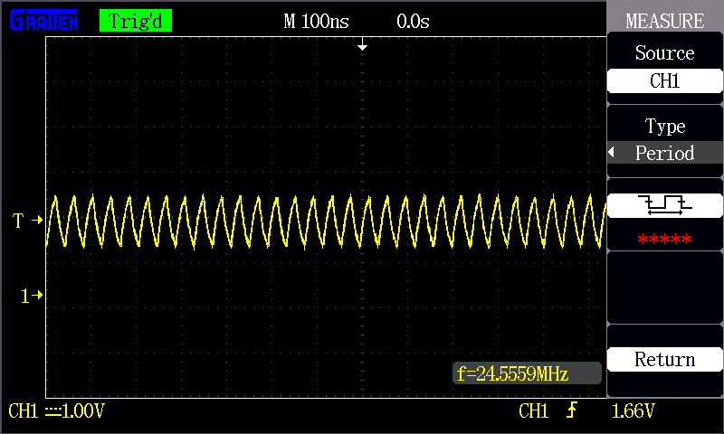
24.576MHz Clock Out
PCB Issues Uncovered
While I was happy that the clocks seemed to be running at the right rate, it was quickly apparent that all was not well with this design. The peak-to-peak voltage seemed pretty compressed, and the waveform was not what I wanted. The PCM5242 datasheet timing requirements for SCK state that the clock must be above & below the logic thresholds of 0.7DVDD (2.31V) and 0.3DVDD (0.99V) for at least 9ns. Just eyeballing the shape of the trace, it looks like this may not be the case. The peak-to-peak voltage seems to be just over 1V, which is a bit too close for comfort. I believe this issue to be due to capacitance caused by my jumpering of the 12MHz clock from one side of the PCB to the other side, then jumpering the 24.576MHz signal back to the original side of the board.
I was able to see some pretty cruddy audio signals on the analog out pins of the board (sadly, I do not have the traces). I believe this to be because the audio PLL was able to occasionally lock, but not for long; the output looked to be discontinuous, which I’d expect in that case.
Next Steps
Good news is that I feel confident that the ins-and-outs of the PCB are roughly correct! I will now re-design the board to try to keep the clock lines clean (i.e. don’t require using 5" of jumper wire). I want to be careful not to introduce noise to the analog side of the board, so I’ll have to be smart about how I select the GPIO pins to use, and how I route the signals.
There is another alternative that I’ve been exploring as well, but I’ll save that for its own blog post. The idea is to replace the USB-2-I2S stage w/my own microcontroller that can output an I2S clock that I can use directly. Long-term, this is what I’ve wanted to do, but originally I wanted to move quickly. However, this requires more hardware changes than I love, and since I need something to configure the I2C registers on the PCM5242 anyways, this might be the time to switch to my own first stage…